
How to Prevent Cracking and Delamination in PCB Fabrication Assembly
Delamination in PCB Fabrication Assembly
A multilayer printed circuit board (PCB) consists of interlinked layers of fiberglass and resin. Cracks or delamination break these layers, reducing functionality and lifespan. Preventing these defects through robust PCB design and manufacturing reduces their likelihood, but unforeseen factors like environmental stressors can still cause them.
Moisture intrusion is the most common cause of PCB delamination. This occurs when moisture gets trapped between layers and expands at high temperatures, such as during soldering or reflow oven baking. Even a small amount of moisture can cause this damage, which may lead to internal or external cracking. Moisture can also trigger conductive anodic filamentation, or CAF, where metallurgical reactions form small filaments of copper between conductors in the PCB. This causes a short circuit, resulting in costly failures and repair costs.
The pcb fabrication assembly process uses FR4 as its base material, which absorbs moisture and can be prone to delamination when exposed to excessive heat. To prevent this, manufacturers must carefully control the lamination and reflow oven processing steps. This includes pre-baking the base materials, ensuring resin controls, and running the reflow oven at the correct temperature.
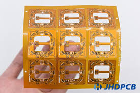
How to Prevent Cracking and Delamination in PCB Fabrication Assembly
Thermal stresses can also contribute to PCB delamination. Repeated cycling of heating and cooling exacerbates differences in thermal expansion and contraction between layer materials, which weakens adhesive bonds over time. Physical flexing of the PCB or constraints on the chassis can concentrate these stresses and cause them to propagate along specific areas of the board. Insufficient bonding, contamination, and uneven resin flow can also create weak points prone to delamination.
A damaged PCB is a costly problem that will require professional PCB repairs to return it to working condition. To minimize these costs, companies can implement prevention best practices like simulation, testing, material selection, and process control to reduce the risk of delamination. Additionally, they can use a PCB manufacturer with a strong track record of providing quality work and fast turnaround times.
Another significant advancement is the use of flexible PCBs. Unlike traditional rigid boards, flexible PCBs can bend and conform to various shapes, making them ideal for applications in medical devices, automotive electronics, and consumer gadgets. Flex-rigid PCBs, which combine both rigid and flexible sections, offer additional versatility, enabling complex designs that would be challenging with traditional rigid boards alone.
If a defect in the board’s construction or handling does occur, the manufacturer can spot-solder jumpers over any voids and apply a conformal coating to protect it from environmental stresses. This can help the board regain its functionality and improve its durability. However, if a delamination is too large or widespread, the board will likely need to be re-plated with copper or replaced altogether. A thorough inspection and re-working process should be conducted to identify the root cause of the delamination and address it permanently. Then, the product can be returned to service. This process should include thorough visual inspections, AOI systems, and reliability tests to ensure the product meets its requirements. This will help companies build their reputations and increase customer satisfaction.