
Factors That Affect the Bend Radius of a Rigid Flex PCB
Bend Radius of a Rigid Flex PCB
Rigid-flex PCBs combine the rigidity of a traditional printed circuit board with a flexible substrate. This combination makes them ideal for applications in which the PCB must be durable, rugged, and able to withstand significant mechanical stress such as repeated bending and flexing. To ensure that a rigid-flex PCB is able to withstand these conditions, engineers must take into account several factors during design and manufacturing processes. These include the thickness and structure of copper layers, the type of dielectric used, stiffeners, and flammability considerations. They must also consider the design of conductors and impedance control.
One important factor is the bend radius of a rigid flex pcb. The bend radius is the minimum amount of space that a PCB can safely bend without causing damage or degrading its performance. There are several methods for calculating the bend radius of a rigid-flex circuit board, ranging from simple guidelines based on PCB thickness to complex formulas that take into account specific materials and bending conditions.
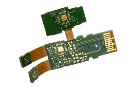
The number of copper layers in a rigid-flex PCB is another key factor that affects its bend radius. Thicker copper layers require larger bend radii than thinner ones, because they are more rigid and less flexible. Additionally, the thickness of the substrate and the type of dielectric material used also influence the bend radius of a PCB.
Factors That Affect the Bend Radius of a Rigid Flex PCB
To ensure that a rigid-flex PCB can withstand repeated bending and flexing, engineers must use the appropriate materials in both the rigid and flexible sections of the board. This includes ensuring that all components have the correct thermal expansion coefficient to prevent cracking and delamination. It is also critical to plan the layout of the rigid and flexible sections of the board carefully, ensuring that all signal paths transition smoothly between the two areas.
In addition, it is critical to avoid placing pads, holes, and vias on the bending region of the circuit board. These areas can apply mechanical stresses that could damage the copper and cause structural failure. Ideally, these features should be placed on the rigid section of the board or at least away from the bending area.
The flexibility of rigid-flex PCBs also enhances reliability by reducing the number of interconnects and solder joints. With fewer points of failure, these boards exhibit superior resistance to mechanical stress, vibration, and thermal cycling. Consequently, rigid-flex PCBs are well-suited for environments characterized by extreme conditions, including automotive electronics, medical implants, and military equipment.
Other important considerations for a rigid-flex PCB include the placement of connectors and the size and location of signals in the flexible zone. Poor connector placement can lead to mechanical stress and may compromise signal integrity or electromagnetic interference (EMI). It is also important to ensure that the rigid and flexible portions of the board are properly matched for temperature and flex-bend sensitivity. Finally, rigorous testing and inspection is necessary for rigid-flex PCBs to verify their integrity and functionality. This requires special flex-testing equipment and procedures.