
How an HDI PCB Differs From a Traditional PCB?
HDI PCB
When you need a PCB for your next electronic project, consider an HDI PCB. This type of board features high-density interconnections that provide higher performance and allow you to cram more capabilities into a smaller space. It’s also less prone to damage from environmental conditions and physical impacts.
An hdi pcb is built using a build-up process that involves very thin laminate cores and pre-preg layers. These are then combined with sequentially bonded copper foil layers to form the multi-layer boards. This technology allows for extremely tight trace spacing and clearances under 4 mils. This is a significant improvement over traditional PCBs, which often have a clearance of up to 8 mils or more.
The design of an hdi pcb requires extra precision due to miniature pads and fine pitch of the circuitry. However, a well-designed board will offer many benefits such as a shorter lead length that reduces power consumption and leads to increased reliability and quality of the circuit. Additionally, the small size of an HDI pcb makes it possible to use less copper, reducing the overall cost and weight of the finished product.
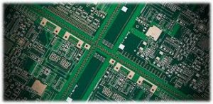
How an HDI PCB Differs From a Traditional PCB?
Typical applications for HDI PCBs include portable electronics such as cell phones, touch-screen devices and laptop computers. They are also used in automotive and aerospace systems to control engine operations, safety features and other functions. In addition, they are employed in industrial automation to relay information between machines and improve efficiency.
As with all PCBs, the choice of materials and design will impact the production costs. For example, selecting the right layer count will affect the amount of time required to complete the lamination and drilling cycles. In addition, the choice of metallization and plating will also play a role in the final cost.
To maximize the performance of your HDI PCB, choose a fabricator that offers a range of manufacturing options. This includes a wide selection of metallizations and finishes. Some reputable manufacturers even offer immersion tin, immersion silver and ENIG options. These options will help you achieve the best possible results and price for your project.
You should also consider the number of layers and via structure types in your HDI design. The choice of these will have a direct impact on the manufacturing cost, especially when using different stack-ups for each of your layer pairs. For example, using different layers for the ground and power planes will allow you to minimize vias in the core by incorporating the shortest possible route between the two. This will lower your power supply impedance and enable you to use smaller traces for better signal integrity.
Finally, a good HDI design will take into account your component packaging requirements. For instance, you may want to use a pinless package for your BGA components or require the smallest footprint possible for your surface mount devices. This will make it easier to install the components and minimize the space they take up on the board. In the end, a well-designed HDI PCB will offer the most reliable and durable electronic products for your customers.