
How do high density interconnects handle vibrations and shocks?
high density interconnects handle vibrations and shocks
High density interconnects enable more components to fit on a PCB, increasing the performance and functionality of devices. They also reduce space requirements, making them ideal for applications where size and weight are crucial. Nevertheless, such PCBs need to be able to handle mechanical vibrations and shocks. Vibrations can cause the PCB to move and shake, which results in a change of position that can cause damage to components and solder joints. It is also possible for the PCB to suffer from abrasions and impact.
Hence, it is important to test the stability of the circuit boards during production and handling. A new generation of test equipment is now available for this purpose. It identifies and sets up sensors automatically, which saves time and eliminates human error. The system can also be set up to use a range of different sensor types. This way, the test can be adapted to the specific needs of the application. The system can calculate the shock response spectrum and display it in real-time or as a plot. It also supports ISO standards for repeatability and compliance. It can even select the appropriate damping ratio or quality factor for the test data based on the user’s specifications.
The latest high density interconnect technology is designed to be more robust against the effects of mechanical vibrations and shocks. This is because it uses microvias with a smaller diameter than through-hole (TH) holes and can also incorporate blind and buried vias. The result is a more compact circuit board with increased signal density and higher-speed data transmission.
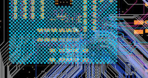
How do high density interconnects handle vibrations and shocks?
It also allows for the mounting of miniature integrated circuits like flip chips and BGAs, which cannot be mounted on conventional PCBs. The use of HDI also means that fewer holes are required, which lowers the overall mass of the device. This is especially significant for applications that require a mobile and lightweight device.
Various factors can influence the stability of the PCB, including temperature, operating loads and the number of connections. Vibrations, impacts and drop tests are common methods of testing for these conditions. However, the most important factors are how the component and circuit board are assembled. Using a high-quality manufacturing process is essential, as it will increase the longevity of the circuit board and its reliability against vibrations and shocks.
The emergence of smart electronics is creating a demand for high-density interconnects, as companies look to maximize the performance and features of their products. To do this, they must be able to fit more components on the same board and mount them at an even tighter pitch. This is why it is essential to work with a PCB manufacturer that uses the latest HDI technology. Moreover, using the right routing rules is critical to optimizing the design of your circuit board. This will improve both the electrical performance and routing efficiency. The right routing rules will also help ensure that your circuit board can withstand a wide range of environments, including harsh conditions such as vibrations and shocks.