
Limitations of Flex Circuit PCBs
Flex Circuit PCBs
As our electronic devices get smaller and more compact, the size and shape of circuit boards must change to keep up with the demands. This has led to innovations like flex circuits, which can help us design and assemble products in a range of shapes and sizes without compromising on functionality. Flexible PCBs can be used for a wide range of applications, including heads-up displays for aerospace piloting and minuscule medical devices that can be inserted into patient bodies. These specialized circuit boards are extremely thin, and have high levels of bendability and tensile strength. They are also capable of delivering a wide range of benefits, from reducing manufacturing costs to improving reliability.
Unlike rigid PCBs, which have thick substrates and copper foil layers, flex circuit pcb are made from a flexible material such as polyimide or polyester. This allows them to be bent a number of times without damaging the insulation layer or copper foil. It also allows the circuit to be molded into more complex three-dimensional shapes, which can be ideal for some applications.
One of the primary limitations of flex circuits is that they do not provide as much mechanical support as rigid PCBs, which can cause damage to the copper and other components in the flex region. As a result, it is important to choose the right flex material for your design and to make sure that the design itself can handle the bending and flexing required of the application.
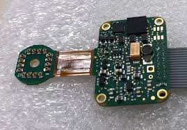
Limitations of Flex Circuit PCBs
The choice of a flex material will depend on the type of conductive material that is chosen for the circuit board, as well as the desired level of flexibility. Copper is commonly used as it provides excellent conductivity, heat resistance, and flexibility. Other conductive materials may include aluminum, silver, and gold. It is critical to consider the thickness of the flex material when designing your circuit board, as this will impact the overall thickness and performance of the resulting product.
In addition to avoiding flex material that is too thin, it is also important to pay close attention to the traces, pads, and vias that are placed in the flex area. For example, it is best to avoid any plated through holes (PTH) in the flex region, as these can be susceptible to abrasion and mechanical stress during assembly and operation. It is also important to choose a no-flow prepreg bonding material that is compatible with the flex and rigid materials. This is generally available in both standard FR-4 and Polyimide, and can help to prevent detachment of the copper from the pad.
Another factor to consider is that flex PCBs require a different approach to pad sizing and etching. For instance, flex pads should be designed with a large enough radius to accommodate the expected bending. In addition, the trace-to-pad spacing should be increased to a minimum of 0.010 inches. This will prevent the exposed copper from sagging and possibly snagging on other components or connectors in the assembly.